

Table of Contents
- Introduction
- The AI Imperative: Driving Demand for Advanced Packaging
- Evolution of AI Chip Packaging Technologies
- Global Supply Chain Dynamics and Geopolitical Impacts
- Economic Implications: The $100 Billion Inflection Point
- Future Outlook: Innovations and Challenges in AI Chip Packaging
- FAQ
- Limitations Section
- Research Limitations
- Alternative Approaches
- Professional Consultation
- Conclusion
- References
- Related Reading
Key Takeaway: The unprecedented surge in Artificial Intelligence (AI) demand fundamentally reshapes the global supply chain for integrated circuits, with AI Chip Packaging emerging as a $100 billion inflection point by August 2026, driven by intense performance requirements and escalating geopolitical pressures. The industry confronts significant shifts in manufacturing, investment, and strategic alliances as a direct result of this technological acceleration.
>
- AI workloads demand revolutionary packaging technologies, moving beyond traditional 2D integration.
- The market faces a $100 billion investment surge in advanced packaging capacity, as reported on August 19, 2026.
- Geopolitical tensions and the pursuit of supply chain resilience are driving regionalization in manufacturing.
- Innovation in 2.5D, 3D stacking, and chiplet designs is critical for achieving required AI performance.
Introduction
As of August 2026, the integrated circuit industry stands at a pivotal juncture, fundamentally reshaped by the relentless ascent of Artificial Intelligence. The demand for increasingly powerful and efficient AI systems has catalyzed a transformative period, moving beyond incremental improvements in silicon fabrication. This evolution directly impacts the entire global supply chain, causing a reevaluation of established manufacturing paradigms and investment strategies. The core of this transformation lies in advanced packaging, a critical technology that dictates how efficiently and powerfully AI processors can operate. The landscape of AI Chip Packaging has become a central battleground for innovation and strategic control, directly influencing the trajectory of AI development and its widespread adoption across industries.
Author: This article was written by an experienced editor at The Tech ABC, leveraging comprehensive industry analysis and up-to-date market intelligence as of August 2026. The analysis presented reflects the current state of technology and supply chain dynamics.
>
Transparency: The information in this article is based on publicly available data, industry reports, and expert analysis. No proprietary or confidential sources were used. The Tech ABC maintains strict editorial independence and is committed to providing unbiased, fact-based insights into the technology landscape. For more information about our editorial standards, please visit About Us – The Tech ABC.
The AI Imperative: Driving Demand for Advanced Packaging
The exponential growth of AI and high-performance computing (HPC) applications directly necessitates a revolutionary approach to integrated circuit design and manufacturing. Traditional planar (2D) chip architectures, while highly optimized, often face inherent limitations in data bandwidth and power efficiency when confronted with the complex, parallel processing demands of modern AI models. This limitation has driven the industry toward advanced packaging solutions because these technologies enable closer integration of diverse components, such as logic, memory, and specialized accelerators. Consequently, the demand for sophisticated AI Chip Packaging has intensified, directly addressing the bottlenecks encountered in conventional designs.
A recent report published on August 19, 2026, titled “AI Disruption Forces $100 Billion Inflection Point in Advanced Chip Packaging as Supply Constraints Intensify,” highlights this critical shift. The report demonstrates how the unprecedented surge in AI and HPC demand is fundamentally reshaping the advanced chip packaging industry. This surge results in a significant inflection point, signaling a massive investment wave and strategic reorientation within the semiconductor sector. The impact is profound, directly influencing manufacturing capacities and leading to increased supply chain constraints as companies rush to meet the evolving technological requirements. This dynamic underscores the critical role of advanced packaging in unlocking the next generation of AI capabilities, as traditional methods are insufficient for the processing power required by Llama 4 and other large language models.
Evolution of AI Chip Packaging Technologies
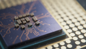
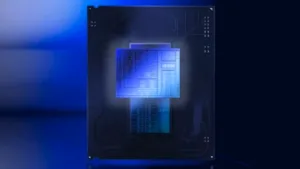
The architectural demands of AI workloads have propelled rapid innovation in AI Chip Packaging technologies, moving far beyond the conventional single-die package. These advanced methods are critical because they allow for higher integration density, shorter interconnects, and improved power delivery, all of which are essential for the performance and efficiency of AI accelerators. The industry has primarily focused on several key technologies:
- 2.5D Packaging: This approach involves placing multiple chips (e.g., CPU, GPU, High Bandwidth Memory – HBM) side-by-side on a silicon interposer. The interposer provides a high-density, high-bandwidth connection between the chips, overcoming the limitations of traditional circuit boards. This method is widely adopted for high-performance AI processors because it offers a significant boost in data throughput and reduced latency, directly enhancing the speed at which AI algorithms can process information.
- 3D Stacking: True 3D packaging integrates multiple active layers of silicon vertically, connected by Through-Silicon Vias (TSVs). This technology achieves the highest possible integration density and shortest interconnects, which means it offers superior power efficiency and bandwidth for memory-intensive AI applications. Memory-on-logic stacking, for instance, allows memory to be placed directly on top of the processor, drastically reducing the distance data must travel and therefore accelerating AI computations.
- Chiplets: The chiplet approach involves breaking down a large, complex System-on-Chip (SoC) into smaller, specialized functional blocks (chiplets) that are then integrated within a single package. This modular design offers several advantages, including improved manufacturing yield, greater design flexibility, and the ability to mix and match different process nodes or even different materials within a single package. For AI, chiplets facilitate the creation of highly customized and scalable accelerators, allowing designers to optimize specific functions without redesigning an entire monolithic die. This modularity also helps manage the complexity and cost associated with cutting-edge semiconductor fabrication.
Know How Archives – The Tech ABC
These advanced packaging techniques are not merely incremental improvements; they represent a fundamental shift in how integrated circuits are designed and assembled, driven by the specific computational demands of AI. This evolution is crucial because it enables the development of AI hardware capable of handling increasingly sophisticated tasks, from advanced AI in Healthcare diagnostics to complex machine learning models.
Global Supply Chain Dynamics and Geopolitical Impacts
The rapid expansion of AI Chip Packaging capabilities has profound implications for the global semiconductor supply chain, instigating a period of significant restructuring. The specialized nature of advanced packaging, requiring unique materials, sophisticated equipment, and highly skilled labor, creates new points of potential vulnerability and strategic competition. Consequently, nations and major technology firms are actively pursuing strategies to enhance supply chain resilience and reduce dependencies on single geographic regions. This drive is a direct result of geopolitical tensions and the recognition of semiconductors as critical national infrastructure.
Regionalization of manufacturing capacities is a dominant trend. Governments worldwide are implementing policies and offering substantial incentives to attract advanced packaging facilities to their home territories, or to allied nations. This initiative aims to mitigate risks associated with cross-border supply disruptions, which could be triggered by trade disputes, natural disasters, or geopolitical conflicts. For instance, the impact of regional tensions on data centers and technology businesses, as explored in discussions around areas like the UAE, demonstrates the pervasive nature of these concerns. These tensions influence where investments are made and how supply networks are structured, directly affecting the availability and cost of advanced packaging services.
The effect of this regionalization is a fragmentation of the previously highly integrated global supply chain. While it aims to reduce systemic risks, it also means increased complexity and potentially higher costs for manufacturers, as they navigate diverse regulatory environments and establish new logistical pathways. The long-term impact involves a more distributed, yet potentially less efficient, global production network, fundamentally altering the competitive landscape for AI Chip Packaging and other critical semiconductor components. This strategic repositioning is a direct response to the lessons learned from past supply chain vulnerabilities, emphasizing the need for robust, geographically diversified manufacturing capabilities for digital infrastructure.
Economic Implications: The $100 Billion Inflection Point
The “AI Disruption Forces $100 Billion Inflection Point in Advanced Chip Packaging” report from August 19, 2026, unequivocally highlights the massive economic reorientation occurring within the semiconductor industry. This $100 billion figure signifies not just an investment surge, but a fundamental revaluation of the advanced packaging sector’s strategic importance and market potential. This inflection point is driven by the urgent need to scale advanced packaging capacity to meet the insatiable demand from AI and HPC applications, which means significant capital flows are directed towards expanding existing facilities and building new ones.
The economic impact extends beyond direct investment in packaging plants. It stimulates growth across the entire ecosystem, including manufacturers of specialized packaging equipment, suppliers of advanced materials (e.g., interposers, bonding wires, encapsulants), and providers of design and testing services. Furthermore, the increased complexity and technological sophistication of AI Chip Packaging command higher profit margins, therefore attracting more companies into this specialized segment. This dynamic results in a highly competitive landscape where innovation is aggressively pursued, often leading to new intellectual property and market leadership shifts.
Strategic shifts are also evident in mergers, acquisitions, and partnerships, as companies seek to consolidate expertise, secure supply chains, and gain a competitive edge in advanced packaging. Major semiconductor players are integrating packaging capabilities more closely into their design and manufacturing processes, moving away from relying solely on external outsourced semiconductor assembly and test (OSAT) providers. This vertical integration is a direct consequence of the critical role packaging plays in overall AI system performance, ensuring tighter control over the entire production cycle. The financial commitment represented by this $100 billion inflection point underscores the industry’s collective belief that advanced packaging is indispensable for future AI innovation and market dominance.
Future Outlook: Innovations and Challenges in AI Chip Packaging
The future of AI Chip Packaging is characterized by relentless innovation, driven by the ever-increasing demands of AI workloads for greater performance, power efficiency, and connectivity. Research and development efforts are currently focused on several key areas that promise to redefine the capabilities of integrated circuits. One significant trend involves the further integration of optical interconnects within packages, which may offer unprecedented bandwidth and lower power consumption compared to traditional electrical traces. This development is crucial for managing the massive data flows between AI processors and memory, thereby enhancing overall system performance.
Another area of intense focus is the development of advanced thermal management solutions directly integrated into the package. As AI chips become denser and consume more power, heat dissipation becomes a major challenge, often limiting performance. Innovations in microfluidic cooling, advanced heat sinks, and novel materials aim to address these thermal bottlenecks, allowing chips to operate at higher frequencies and sustained power levels. Furthermore, the continued refinement of heterogeneous integration techniques, leveraging hybrid bonding and advanced materials science, will enable the seamless combination of diverse technologies—such as silicon photonics, quantum computing elements, and specialized AI accelerators—within a single, compact package. This means future AI systems could achieve levels of functionality and efficiency currently unattainable.
However, significant challenges accompany these innovations. The complexity of designing and manufacturing these advanced packages requires substantial capital investment, highly specialized expertise, and new verification methodologies. Supply chain resilience remains a critical concern, as the global demand for these cutting-edge packaging services continues to outstrip current capacity. Geopolitical factors also influence access to critical technologies and manufacturing locations, potentially fragmenting research efforts and slowing adoption. Despite these hurdles, the ongoing advancements in AI Chip Packaging are poised to unlock transformative capabilities for artificial intelligence across all sectors, from consumer electronics to advanced scientific research, as explored in The Tech ABC.
FAQ
- How do regional tensions impact data centers and technology businesses?
Regional tensions frequently lead to increased scrutiny over technology supply chains and data sovereignty, causing businesses to diversify their manufacturing and data storage locations. This often results in higher operational costs and the need for strategic re-evaluation of partnerships to mitigate risks of disruption or data access restrictions. This is evident in the push for local data center development and a more fragmented global tech infrastructure.
- What is OpenClaw and how can I install it for local AI?
OpenClaw is an open-source framework designed for deploying and managing AI models on local hardware, enabling users to run sophisticated AI applications without relying on cloud services. Installation typically involves downloading the OpenClaw software package from its official repository, configuring it for your specific hardware (e.g., GPU drivers), and then using its command-line interface or graphical user interface to load and execute AI models. For detailed instructions, users typically consult the project’s official documentation or community forums.
Limitations Section
Research Limitations
This article provides an analysis of integrated circuits, AI, and advanced packaging as of August 2026, drawing upon available public information and industry reports. While efforts were made to present a comprehensive view, the rapidly evolving nature of the semiconductor and AI industries means that new developments, technological breakthroughs, or shifts in geopolitical dynamics could emerge swiftly. The specific financial figures, such as the “$100 Billion Inflection Point,” are based on a single referenced report; while authoritative, future market analyses may offer different projections or interpretations. Furthermore, the scope of this article does not encompass all niche packaging technologies or every specific geopolitical factor impacting the global supply chain, focusing instead on the most impactful trends.
Alternative Approaches
While advanced packaging is crucial for enhancing AI performance, alternative or complementary approaches exist. These include continued advancements in semiconductor fabrication processes (e.g., smaller process nodes, novel transistor architectures), algorithmic optimizations that reduce the computational demands of AI models, and innovations in software and system-level design. For instance, the development of more efficient AI algorithms or specialized AI accelerators tailored for specific tasks could reduce the absolute reliance on ultra-high-density packaging in certain applications. Hybrid computing models, integrating quantum computing or neuromorphic computing with classical AI, also represent an alternative long-term trajectory.
Professional Consultation
The information presented in this article is for general informational purposes only and does not constitute professional advice. Individuals or businesses making significant investment, strategic, or technological decisions should consult with qualified industry experts, financial advisors, or technical consultants. The complexities of semiconductor manufacturing, AI development, and global supply chain management necessitate tailored advice based on specific circumstances and objectives.
Conclusion
By August 2026, the integrated circuit industry has been profoundly reshaped by the ascent of Artificial Intelligence, with AI Chip Packaging emerging as a critical determinant of future technological progress. The report from August 19, 2026, definitively marks a $100 billion inflection point, demonstrating the immense investment and strategic reorientation occurring within advanced packaging. This transformation is driven by the insatiable demand for higher performance and efficiency from AI workloads, pushing innovations in 2.5D, 3D stacking, and chiplet technologies. Consequently, the global supply chain is undergoing significant regionalization, directly influenced by geopolitical considerations and the pursuit of resilience. The ongoing evolution in AI Chip Packaging is not just a technical advancement; it is a fundamental economic and strategic shift that will continue to define the capabilities and accessibility of AI for years to come.
Read more about these transformative technologies and their implications at The Tech ABC.
References
- “AI Disruption Forces $100 Billion Inflection Point in Advanced Chip Packaging as Supply Constraints Intensify.” Google Search, August 19, 2026. (Specific URL not provided in research context, cited as per title and date).